Scanning Electron Microscopy (SEM) is based on the principle of using a focused beam of high-energy electrons to probe the surface of a sample and produce a high-resolution detailed image.
Electron Source: SEM works by using an electron source, typically a heated tungsten filament or a field emission gun, to produce a beam of electrons.
Electron Beam Generation: The electron source emits electrons, which are accelerated to high energies by an electric field. The electrons are focused into a narrow beam using electromagnetic lenses.
Sample Interaction: The primary electron beam is directed onto the sample's surface. When the beam interacts with the sample, several types of interactions occur, including scattering, absorption, and emission of secondary electrons.
Scattering: The primary electrons may undergo elastic or inelastic scattering while interacting with the atoms in the sample. Elastic scattering results in a change in direction of the electron beam, while inelastic scattering leads to energy loss due to interactions with the sample's atoms.
Secondary Electron Emission: Some of the primary electrons knock off secondary electrons from the surface of the sample through inelastic scattering. These secondary electrons carry information about the sample's topography and composition.
Signal Detection: The emitted secondary electrons, along with other signals such as backscattered electrons and characteristic X-ray emissions, are detected using various detectors. Some common detectors in SEM are the Everhart-Thornley detector for secondary electrons and detectors for backscattered electrons or X-rays generated by the sample.
Image Formation: The detected signals are then amplified and processed to form an image. The signal intensity is typically converted into a grayscale or false-color representation, allowing the visualization of surface features and details.
Scanning: To generate a complete image, the electron beam is systematically scanned across the surface of the sample in a raster pattern. The intensity of the detected signals at each point is recorded, allowing the construction of a high-resolution image.
Image Display and Analysis: The final reconstructed image is displayed on a monitor or recorded for further analysis. SEM images can be used to examine the microstructure, morphology, elemental composition, and surface characteristics of a wide range of materials.
In short, scanning electron microscopy utilizes the interaction of a focused, high-energy electron beam with a sample to generate detailed images. By analyzing the signals emitted by the sample, SEM provides valuable information about the surface topography, morphology, and composition of the sample at high resolution. It is widely used in a variety of scientific and industrial applications for research, quality control, and materials characterization.
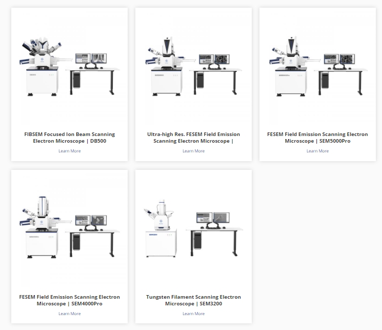
CIQTEK offers various high-quality SEM equipment for researchers and industrial users.
